
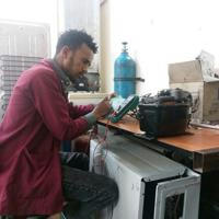
HOME Electromechanical Solution
#Electromechanical service #washing machine ጥገና #Refrigerator #micro wave Oven #tv ጥገና #የሻይ:የዳቦ:ሊጥ ማቡኪያ ማሽን ጥገና #የቢሮ ማሽኖችና የ security ካሜራ #cctv ገጠማና ጥገና # አጠቃላይ ኤሌክትሪክ መስመር ዝርጋታዎች ''ችግር ፈቺ እንጂ ችግር ፈጣሪ አንሁን'' call us +251923997025 +251960903217
Mostrar más487
Suscriptores
Sin datos24 horas
-27 días
-330 días
- Suscriptores
- Cobertura postal
- ER - ratio de compromiso
Carga de datos en curso...
Tasa de crecimiento de suscriptores
Carga de datos en curso...
UNDERSTANDING
October 27, 2020 by darla.india
Darla:
L.C.D L.E.D T.V Panels Connection and Voltages Understanding
Here we talking about the main voltages and pin connection of L.C.D and L.E.D T.Vs
Panels, every technician should know where to test and how to check voltages of each connection as they mention in Service Manual or schematic diagram or at least you should know the basic working voltages.
Connection Name Connection Working Voltages
1. VGL in Driver negative P.supply1 Around -10.5v
2. VCL in Driver negative p.supply2 Around -10v to -12v
4. VDD VDD is the logic supply input for the scan driver.
5. VGH Supply LCM driver output Around 12v+ to 19.5v+
6. STV Vertical Sync Input. The rising edge of STV begins a frame of data. The STV input is used to generate the high-voltage STVP output. PulseL.C.D L.E.D T.V Panels Connection and Voltages Understanding
Here we talking about the main voltages and pin connection of L.C.D and L.E.D T.Vs
Panels, every technician should know where to test and how to check voltages of each connection as they mention in Service Manual or schematic diagram or at least you should know the basic working voltages.
6. STV Vertical Sync Input. The rising edge of STV begins a frame of data. The STV input is used to generate the high-voltage STVP output. Pulse
7. CPV1 Vertical Clock-Pulse Input. CPV1 controls the timing of the CKV1 and CKVB1 outputs, which change state (by first sharing charge) on its falling edge.
Pulse
8. CPV2
9. V.COM out Vertical Clock-Pulse Input. CPV2 controls the timing of the CKV2 and CKVB2 outputs, which change state (by first sharing charge) on its falling edge.
Common signal output TFT Clock pulse
Signal pulse
10. POL in Supply input common signal Signal
11. VDC in Supply +5.0v min
12. VON Gate-On Supply. VON is the positive supply voltage for the CKV_, CKVB_, and STVP high-voltage driver outputs. Around 20v+
13. V-OFF Gate-Off Supply. VOFF is the negative supply voltage for the CKV_, CKVB_, and STVP high-voltage driver outputs. Around 8V-
Brief Details of Panels Connection Points
VDD VDD is the logic supply input for the scan driver.
VON Gate-On Supply. VON is the positive supply voltage for the CKV_, CKVB_, and STVP high-voltage driver outputs.
VOFF Gate-Off Supply. VOFF is the negative supply voltage for the CKV_, CKVB_, and STVP high-voltage driver outputs.
STV Vertical Sync Input. The rising edge of STV begins a frame of data. The STV input is used to generate the high-voltage STVP output.
CPV1 Vertical Clock-Pulse Input. CPV1 controls the timing of the CKV1 and CKVB1 outputs, which change state (by first sharing charge) on its falling edge.
CPV2 Vertical Clock-Pulse Input. CPV2 controls the timing of the CKV2 and CKVB2 outputs, which change state (by first sharing charge) on its falling edge.
EN Enables the MAX17121. Drive EN high to start up the MAX17121 after a delay time, which is set by a capacitor at DLY.
CKVB1 High-Voltage Scan-Drive Output. CKVB1 is the inverse of CKV1 during active states and is high impedance whenever CKV1 is high impedance.
CKVB2 High-Voltage Scan-Drive Output. CKVB2 is the inverse of CKV2 during active states and is high impedance whenever CKV2 is high impedance.
CKVBCS2 CKVB2 Charge-Sharing Connection. CKVBCS2 connects to CKVCS2 whenever CPV2 and STV are both low (to make CKV2 and CKVB2 high impedance) to allow CKV2 to connect to CKVB2, sharing charge between the capacitive loads on these two outputs.
CKVCS2 CKV2 Charge-Sharing Connection. CKVCS2 connects to CKVBCS2 whenever CPV2 and STV are both low (to make CKV2 and CKVB2 high impedance) to allow CKVB2 to connect to CKV2, sharing charge between the capacitive loads on these two outputs.
STVP High-Voltage Scan-Drive Output. STVP is connected to VOFF when STV is low and is connected to VON when STV is
What is SDA or Serial Data, and CLK / SCL or Serial Clock Signal in a Digital Electronic Circuit?
We have noticed that televisions, the latest audio devices, Bluetooth devices, WiFi devices, and various digital devices have SDA and CLK or SCL written in specific places on their circuit boards. For example, SD and CLK or SCL are written near the two pins of the TV's digital tuner, and SD and CLK / SCL are reported near the two pins of the memory IC. This SD stands for Serial Data Signal and CLK / SCL stands for Serial Clock Signal. (posted in the world of electronics group)
What is SDA or serial data signal in a digital circuit?
A serial data signal in a digital circuit refers to transmitting data where individual bits of information are sent one after another along a single communication channel. This contrasts with parallel data transmission, where multiple bits are sent simultaneously through separate channels. In a serial data signal, the bits are typically transmitted using a clock signal that synchronizes the sender and receiver devices. The data is serialized, converted into a stream of bits, and sent sequentially. This method is commonly used in various communication systems, such as USB, Ethernet, SPI (Serial Peripheral Interface), I2C (Inter-Integrated Circuit), and serial ports. Serial transmission allows for more extended distances of communication and is often more cost-effective in terms of cabling because it requires fewer wires than parallel transmission. However, it generally operates at slower speeds than parallel transmission for transferring the same amount of data.(posted in the world of electronics group)
What is a CLK / SCL or serial clock signal in a digital circuit?
In digital circuits, the serial clock (often called CLK / SCL) is a signal-synchronizing data transfer between various components or devices in a Digital Circuit. It is a rhythmic signal that controls the timing of sending or receiving bits of information within a circuit. The CLK / SCL signal ensures that the data sender and receiver operate at the same speed and allows accurate and synchronized communication.
The functionality of the serial clock (SCL) signal is significant in serial communication, where data is transmitted one bit at a time.
Digital devices that communicate serially use the rising (leading edges) or falling edges of the clock signal [see figure below] to determine when to read or change the state of the data being sent or received. This synchronization ensures that the sender and receiver are compatible, preventing data loss or corruption by enabling them to process information simultaneously.
Posted in world of electronics group
In essence, the serial clock (CLK / SCL) signal acts as a metronome for the circuits of digital devices, ensuring that data is sent and received in a coordinated and organized manner while maintaining the integrity and accuracy of the information being transmitted and received,( posted in world of electronics group)
T-CON board is also called logic board or control board. T-CON is the English abbreviation of Timing Controller, which means timing control circuit. At present, there are not many T-CON boards in China, CRT TVs have a history of several decades. The traditional CRT television works by scanning and the signals are serial. The current television standard is based on CRT TV, so the television signal passes through the main board of the television. The output after decoding is also a serial signal. We know that the liquid crystal display works in matrix display mode and processes parallel signals. That is to say, if the TV signal decoded by the motherboard is sent directly to the LCD screen, the LCD screen cannot be displayed. There must be a device that converts serial signals into parallel signals so that the LCD can display TV signals, that's why there is a T-CON board, which is a device that converts serial signals into parallel signals. The TV signal output by the main board is disassembled and recombined on the T-CON board to finally form the control signal and data signal required for row and column drive of the liquid crystal display. The overall circuit of the T-CON board can be roughly divided into three parts: signal processing circuit (main IC and its peripheral circuits), gray scale forming circuit (GMA forming circuit) and power supply circuit (DC/DC circuit). The signal processing circuit mainly converts the TV signal transmitted from the motherboard into control signal, pixel signal, auxiliary signal, etc., required for the LCD screen; The grayscale forming circuit mainly forms the grayscale signal required for the LCD screen (grayscale can make the LCD screen have more layers, making the screen richer and more vivid). The power supply circuit mainly forms the signal processing IC, the power supply voltage of the row driver and the column driver, and the switching voltage of the TFT (TFT turn-on voltage VGH, turn-off voltage of TFT VGL), etc. published in the electronics world group
Photo unavailableShow in Telegram
😎Ethiosat Nss 57°e ተጠቃሚዎች KANA Tv ከተቋረጠባቹ Symbol rate ቀይሮ ስለሆነ እዛው ባለበት በ ሪሞታቹ Menu Installation Antenna Setup Tp List በመግባት Symbol Rate መቀየር 11545 H 45000 አድርጋቹ በ ሪሞታቹ Search አድርገት ወይም Save ብላቹ ስቶጡ ይከፍትላቹሀል።
አዲሱ Frequency 👉11545 H 45000
https://t.me/Heni_Dish_Info
⚠️ለብዙዎቻቹህ ጥያቄ መልስ Kana tv እና በSD ሪሲቨር ላይ የሚገቡ ፍሪኩዌንሲዎች አይኖሩም ስለዚህ ከዚህ በኋላ ግዴታ HD ሪሲቨር መቀየር ይኖርባቹሀል።
WORLD OF ELECTRONICS:
PANEL VOLTAGE UNDERSTANDING
October 27, 2020 by darla.india
Darla:
L.C.D L.E.D T.V Panels Connection and Voltages Understanding
Here we talking about the main voltages and pin connection of L.C.D and L.E.D T.Vs
Panels, every technician should know where to test and how to check voltages of each connection as they mention in the Service Manual or schematic diagram or at least you should know the basic working voltages.
Connection Name Connection Working Voltages
1. VGL in Driver negative P.supply1 Around -10.5v
2. V C L in Driver negative p.supply2 Around -10v to -12v
3. VSS Digital ground GND
4. VDD VDD is the logic supply input for the scan driver.
5. VGH Supply LCM driver output Around 12v+ to 19.5v+
6. STV Vertical Sync Input. The rising edge of STV begins a frame of data. The STV input is used to generate the high-voltage STV P output. PulseL.C.D L.E.D T.V Panels Connection and Voltages Understanding
Here we are talking about the main voltages and pin connection of L.C.D and L.E.D T.Vs
Panels, every technician should know where to test and how to check voltages of each connection as they mention in the Service Manual or schematic diagram or at least you should know the basic working voltages.
Connection Name Connection Working Voltages
1. VGL in Driver negative P.supply1 Around -10.5v
2. V C L in Driver negative p.supply2 Around -10v to -12v
3. VSS Digital ground GND
4. VDD VDD is the logic supply input for the scan driver.
5. VGH Supply LCM driver output Around 12v+ to 19.5v+
6. STV Vertical Sync Input. The rising edge of STV begins a frame of data. The STV input is used to generate the high-voltage STV P output. Pulse
7. CPV1 Vertical Clock-Pulse Input. CPV1 controls the timing of the CKV 1 and CKV B1 outputs, which change state (by first sharing charge) on its falling edge.
Pulse
8. CPV2
9. V. COM out Vertical Clock-Pulse Input. CPV2 controls the timing of the CKV2 and CKV B2 outputs, which change state (by first sharing charge) on its falling edge.
Common signal output TFT Clock pulse
Signal pulse
10. POL in Supply input common signal Signal
11. VDC in Supply +5.0v min
12. VON Gate-On Supply. VON is the positive supply voltage for the CKV_, CKV B_, and STV P high-voltage driver outputs. Around 20v+
13. V OFF Gate-Off Supply. V OFF is the negative supply voltage for the CKV_, CKV B_, and STV P high-voltage driver outputs. Around 8V-
Brief Details of Panels Connection Points
VDD VDD is the logic supply input for the scan driver.
VON Gate-On Supply. VON is the positive supply voltage for the CKV_, CKV B_, and STV P high-voltage driver outputs.
V OFF Gate-Off Supply. V OFF is the negative supply voltage for the CKV_, CKV B_, and ST VP high-voltage driver outputs.
STV Vertical Sync Input. The rising edge of STV begins a frame of data. The STV input is used to generate the high-voltage ST VP output.
CPV1 Vertical Clock-Pulse Input. CPV1 controls the timing of the CKV 1 and CKV B1 outputs, which change state (by first sharing charge) on its falling edge.
CPV2 Vertical Clock-Pulse Input. CPV2 controls the timing of the CKV2 and CKVB2 outputs, which change state (by first sharing charge) on its falling edge.
EN Enables the MAX17121. Drive EN high to start up the MAX17121 after a delay time, which is set by a capacitor at DLY.
CKV B1 High-Voltage Scan-Drive Output. CKV B1 is the inverse of CKV 1 during active states and is high impedance whenever CKV 1 is high impedance.
CKVB2 High-Voltage Scan-Drive Output. CKVB2 is the inverse of CKV2 during active states and is high impedance whenever CKV2 is high impedance.
CKVBCS2 CKVB2 Charge-Sharing Connection. CKVBCS2 connects to CKVCS2 whenever CPV2 and STV are both low (to make CKV2 and CKVB2 high impedance) to allow CKV2 to connect to CKVB2, sharing charge between the capacitive loads on these two outputs.
አሁን ላይ አጠቃላይ የማቀዝቀዣ ኢንዱስትሪ በሀገሪቱ ጥሩና አዋጭ የገቢ ምንጭ እየሆኑ መተዋል። ለዚህም አሁን ካለው ቴክኖሎጂ ጋር ወደፊት መራመድ ያስፈልጋል ።
እኛም በዘርፉ የለነው እራሳችንን በየዕለቱ በዕውቀትም በልምድም ታድሰን መገኘት አለብን ብዬ አስባለው ።
ለዚህም ሲባል በአይነቱ ልዩ የሆነ ለ 7ተኛ ጊዜ የሚሰጥ የ አጠቃላይ የፍሪጅ ጥገና ስልጠና
ተዘጋጅቷል ።
በ ስልጠናው የተካተተው
🛠BASIC ELECTRONICS
🛠 BASIC REFRIGERATOR concept
🛠 cycle &all fault repair
🛠all brand invertor board
🛠all brand liner invertor board
🛠all brand micom control refrigerator repair
ያጠቃልላል ።
ሁሉም ስልጠናዎች በ 4 ክፍል ተከፋፍሎ ይሰጣል።
ኮርሱም ሚሰጠው በ ቪዲዮ ተሰርቶ ሲሆን ቪዲዮው በ Telegram vip channel ይለቀቃሉ ።
ክፍለ ሀገር ላላችሁ ደግሞ በ usb disk በ ፖስታ ወይም በመኪና እንልካለን ።
ስለዚህ ኮርሱን መውሰድ የምትፈልጉ በ አንድ ጊዜ ክፍያ 3000 ብር
በሁለት ጊዜ የምትፈልጉ 1500 ብር
በመክፈል መውሰድ ትችላላችሁ ።
📘awash bank
01335179579500
Gelana birhanu
📘Commercial bank of Ethiopia
1000459528443
Gelana birhanu
በላይ በተጠቀሰው ሂሳብ ቁጥሮች በመክፈል የደረሰኝ ፎቶ በ telegram inbox @geluLG በመላክ ኮርሱን መውሰድ ትችላላችሁ ።
ለማንኛውም ጥያቄ
+251923997025
+251960903217 መደወል ይቻላል ።
🔆🌼መልካም አዲስ ዓመት🌼🔆
አዲስዓመት
መልካምአዲስዓመት
መልካም አዲስዓመት
መልካም አዲስዓመት
መልካም አዲስዓመት
መልካም አዲስዓመት
አዲስዓመት
አዲስዓመት
አዲስዓመት
አዲስዓመት
አዲስዓመት
አዲስዓመት
አዲስዓመት
አዲስዓመት
አዲስዓመት
አዲስዓመት አዲስዓመት
አዲስዓመትአዲስዓመትአዲስዓመት
አዲስዓመትአዲስዓመትአዲስዓመት
አዲስዓመት
መልካምአዲስዓመት
መልካምአዲስዓመትአዲስዓመት
አዲስዓመት አዲስዓመት
አዲስዓመት አዲስዓመት
አዲስዓመት አዲስዓመት
አዲስዓመት አዲስዓመት
አዲስዓመት አዲስዓመት
አዲስዓመት አዲስዓመት
አዲስዓመት አዲስዓመት
አዲስዓመት አዲስዓመት
አዲስዓመት አዲስዓመት
መልካም አዲስዓመትአዲስዓመት
መልካምአዲስዓመትስዓመት
መልካምአዲስዓመት
አዲስዓመት
ዓመት
አዲስዓመት
መልካምአዲስዓመት
አዲስዓመት
አዲስዓመት
አዲስዓመት
አዲስዓመት
አዲስዓመት
አዲስዓመት
አዲስዓመት
አዲስዓመት
አዲስዓመት
አዲስዓመት
አዲስዓመት
አዲስዓመትመልካምአዲስዓመት
አዲስዓመትመልካምአዲስዓመት
አዲስዓመትመልካምአዲስዓመት
አዲስዓመት
መልካምአዲስዓመት
መልካምአዲስዓመትአዲስዓመት
አዲስዓመት አዲስዓመት
አዲስዓመት አዲስዓመት
አዲስዓመት
አዲስዓመት
አዲስዓመት
አዲስዓመትመልካምአዓመት
መልካምአዲስዓመትአዲትዓመት
አዲስዓመት አዲስዓመት
አዲስዓመት አዲስዓመት
አዲስዓመት አዲስዓመት
አዲስዓመት አዲስዓመት
አዲስዓመት አዲስዓመት
መልካም አዲስዓመትአዲስዓመት
መልካምአዲስዓመትስዓመት
መልካምአዲስዓመት
አዲስዓመት
🔆🔆🔆🔆🔆🔆🔆🔆🔆🔆🔆🔆🔆
🔆🌼🌼🌼🌼🌼🌼🌼🌼🌼🌼🌼🔆
🔆🌼🔸🔸🔸🔸🔸🔸🔸🔸🔸🌼🔆
🔆🌼🔸🕊🌻🌻🌻🌻🌻🕊🔸🌼🔆
🔆🌼🔸🌻🌻 መልካም 🌻🌻️🔸🌼🔆
🔆🌼🔸🌻🌻 አዲስ 🌻🌻🔸🌼🔆
🔆🌼🔸🌻🌻 ዓመት 🌻🌻️🔸🌼🔆
🔆🌼🔸🌻️🌹🌾🌻💐🌹🌻🔸🌼🔆
🔆🌼🔸🕊🌻🌻🌻🌻🌻️🕊🔸🌼🔆
🔆🌼🔸🔸🔸🔸🔸🔸🔸🔸🔸🌼🔆
🔆🌼🌼🌼🌼🌼🌼🌼🌼🌼🌼🌼🔆
👍 1
Elige un Plan Diferente
Tu plan actual sólo permite el análisis de 5 canales. Para obtener más, elige otro plan.